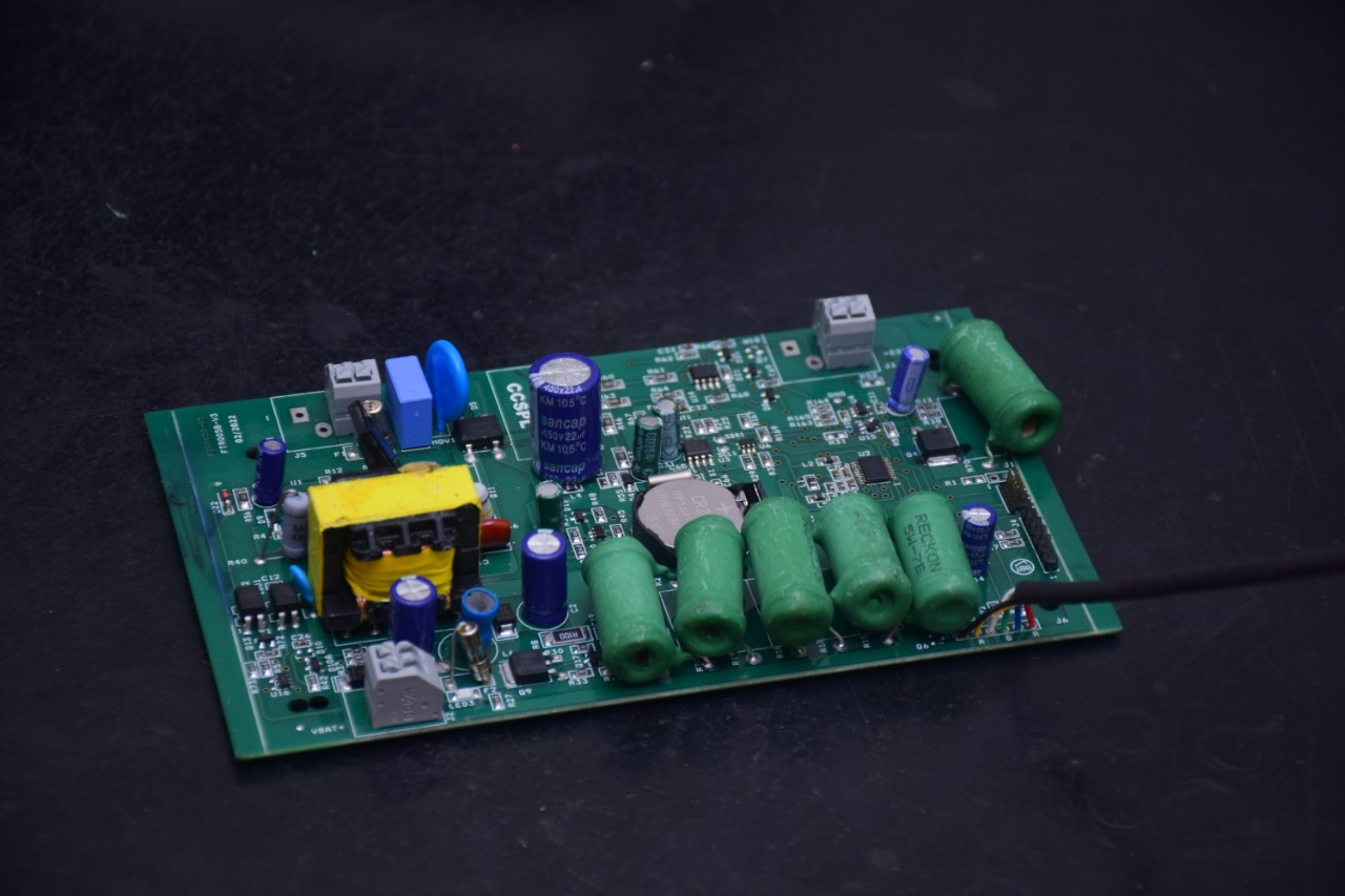
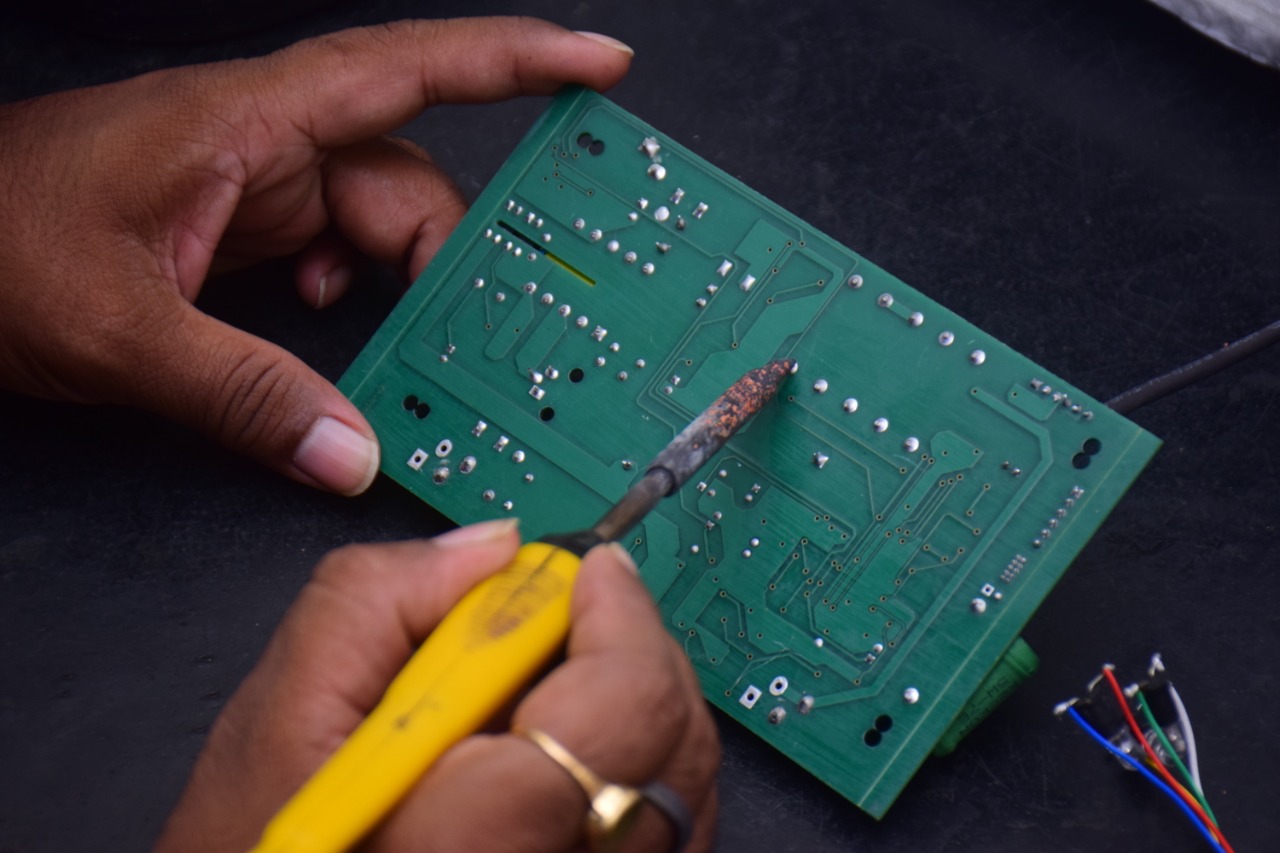
PCB manufacturing process
Our PCB Manufacturing Process includes the following steps :
Step 1 : Data Preparation.
Step 2 : Plotter.
Step 3 : Print inner layers for multilayer PCB.
Step 4 : Plating Through Holes.
Step 5 : Yellow Room.
Step 6 : Electroplating.
Step 7 : Etching & Striping.
Step 8 : Liquid Photo Imaginable.
Step 9 : Nomenclature (Legend).
Step 10 : Routing
Step 11 : Electrical Testing
Step 12 : Final Inspection / Quality Control